skip to main content

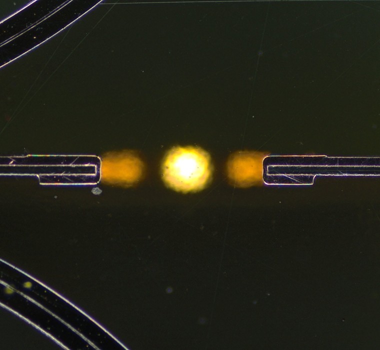
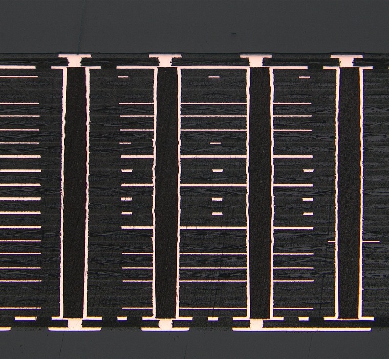
Entdecken Sie die Möglichkeiten von Varioprint

Varioprint steht für innovative Leiterplattentechnologie auf höchstem Niveau. Wir bieten eine breite Palette an Lösungen, Technologien und Materialien, um die anspruchsvollsten Anforderungen zu erfüllen. Erfahren Sie gleich hier mehr über unsere umfangreichen Möglichkeiten oder laden Sie unsere detaillierte Dokumentation herunter.

Products

High Frequency
Flex/Rigid flex
Metal back
Multilayer and HDI
Single- and Double-sided
Special technologies
Electro-Optical Circuit Board (EOCB)

Surfaces

ENIG, ENEPIG, EPIG, DIG
Immersion Silver
Immersion Tin
Electroplate Gold
OSP
Lead free HASL
DIG

Materials

6 FR4
2 High Speed FR4
3 High TG FR4
5 Polyimide Woven Glass
4 Polyimide flex
1 Large selection of HF substrates

Certifications

ISO 9001
ISO 14001
AS 9100
ITAR certified

Specification

Plating
Plating
Standard
Special
Plating
Etching tolerance (in relation to copper layer thickness)
Standard
± 20μm
Special
± 10μm
Plating
Maximum copper layer thickness (Cladding and plated copper)
High surface copper thickness can require multiple solder mask process iterations in order to ensure sufficient solder mask coverage on traces and trace-edges.
Standard
210μm
Special
400μm
Plating
Aspect Ratio depth : through hole Ø
Standard
12:1
Special
15:1
Plating
Aspect Ratio depth : blind via Ø
Standard
1:1
Special
1:1.3
Surface
Surface
Thickness
solderable
bondable
Solder life time
Surface
Electroless Nickel Immersion Gold (ENIG)
Thickness
Ni 3.0 – 7.0µm Au 0.05 – 0.11µm
solderable
Yes
bondable
Yes
Solder life time
12 Months
Surface
Chemical Palladium – Immersion Gold (ENEPIG)
Thickness
Ni: 3.0 – 7.0µm Pd 0.08 – 0.25µm Au 0.03 – 0.08µm
solderable
Yes
bondable
Yes
Solder life time
12 Months
Surface
Electroless Palladium – Reductive Gold (EPIG) (No Nickel surface – good for RF)
Thickness
Pd 0.10 – 0.20µm Au 0.10 – 0.20µm
solderable
Yes
bondable
Yes
Solder life time
12 Months
Surface
Reductive (chemical) Gold
Thickness
Ni 3.0 – 8.0µm Au 0.40 – 0.60µm
solderable
Yes
bondable
Yes
Solder life time
12 Months
Surface
Electroplate Bond Gold
Thickness
Ni 3.0 – 7.0µm Au 0.05 – 0.11µm
solderable
Yes
bondable
Yes
Solder life time
12 Months
Surface
Lead free HASL
Thickness
1 – 30µm
solderable
Yes
bondable
No
Solder life time
12 Months
Surface
Immersion Tin
Thickness
0.8 -1.10µm
solderable
Yes
bondable
No
Solder life time
6 Months
Surface
Immersion Silver
Thickness
0.15 – 0.45µm
solderable
Yes
bondable
No
Solder life time
6 Months
Surface
OSP
Thickness
0.25 – 0.50µm
solderable
Yes
bondable
No
Solder life time
6 Months
Surface
Electroplate Hard Gold (Connector Gold)
Thickness
Ni 3.0 – 8.0µm Au 0.8 – 3.0µm
solderable
Not suitable for soldering or bonding
bondable
Solder life time
Surface
Direct Immersion Gold (DIG)
Thickness
Au 0.2 – 0.3µm
solderable
Yes
bondable
Yes
Solder life time
6 Months
Production panel dimension
Standard
Production panel dimension
Usable area on smallest panel
Standard
265 x 419mm
Production panel dimension
Usable area on middle size panel
Standard
420 x 569mm
Production panel dimension
Usable area on large panel
Standard
490 x 569mm
Production panel dimension
Maximum PCB dimension (single/double sided only)
Standard
569 x 1180mm
Line / Space
Line / Space
Standard
Special
Line / Space
Inner layer (trace width / distance)
Standard
75µm / 75µm
Special
50µm / 50µm
Line / Space
Outer layer (trace width / distance)
Please see also chapter Technology - Fine line
Standard
75µm / 75µm
Special
50µm / 50µm
Laser
Laser
Standard
Special
Laser
µVia ratio depth vs diameter
Standard
1:1
Special
One request
Laser
µVia drill diameter
Standard
100 - 250µm
Special
50 - 100µm
Laser
µVia pad diameter
Standard
300µm
Special
250µm
Mechanics
Mechanics
Standard
Special
Mechanics
Minimum drill diameter
Standard
120μm
Special
75μm
Mechanics
Misalignment 1st tooling drill pattern
Standard
± 30μm
Special
± 20μm
Mechanics
Misalignment 2nd tooling drill pattern
Standard
± 100μm
Special
± 30μm
Mechanics
Misalignment drill – conductor pattern
Standard
± 50μm
Special
± 50μm
Mechanics
Drill depth: through hole Ø
Standard
8:1
Special
14:1
Mechanics
Drill depth: blind hole Ø
Standard
1:1
Special
1:1.3
Mechanics
Outline route (X – Y Axis)
(depending on PCB dimension)
Standard
± 50µm to ± 300μm
Special
± 50µm to ± 200μm
Mechanics
Misalignment routing – drill pattern
Standard
± 150μm
Special
± 50μm
Mechanics
Misalignment routing – conductor
Standard
± 150μm
Special
± 50μm
Mechanics
Misalignment scoring (30° Angle) to drilling
Standard
± 150μm
Special
± 150μm
Plugging
Plugging
Standard
Special
Plugging
Minimum diameter PTH
Standard
0.150mm
Special
One request
Plugging
Maximum diameter PTH
Standard
1.0mm
Special
One request
Plugging
Blind Via depth (IPC related)
Standard
0.5mm class II
Special
0.4mm class III
Plugging
Minimum PCB thickness
Standard
0.2mm
Special
One request
Plugging
Maximum PCB thickness
Standard
4.0mm
Special
On request
Plugging
Selective plugging
Standard
available on request
Special
available on request
Plugging
Plugging paste
Standard
Tayio THP 100 DX1
Special
Tayio THP 100 DX1
Solder mask and Surface protection
Standard
Special
Solder mask and Surface protection
Minimum clearance Solder mask – conductor pattern
Standard
80μm
Special
50μm
Solder mask and Surface protection
Minimum solder mask bar between pads
Standard
80μm
Special
50μm
Solder mask and Surface protection
Minimum solder mask thickness over conductor edge
Standard
5 - 7μm (according to IPC-SM-840)
Special
5 - 7μm (according to IPC-SM-840)
Solder mask and Surface protection
Minimum distance between conductor pattern and assembly print
Standard
150μm
Special
100μm
Solder mask and Surface protection
Minimum symbol height of legend ink
Standard
800µm
Special
500µm
Solder mask and Surface protection
Minimum symbol width of legend ink
Standard
120µm
Special
100µm
Solder mask and Surface protection
Solder mask rigid PCB‘s
Standard
Peters Elpemer SD 2467
Special
Peters Elpemer SD 2467
Solder mask and Surface protection
Solder mask flex PCB’s
Standard
Peters Elpemer SD 2463
Special
Peters Elpemer SD 2463
Solder mask and Surface protection
Printed coverlay and / or stiffener
Standard
available
Special
available
Solder mask and Surface protection
Serialization and traceability down to the individual PCB
Standard
yes barcode and data matrix available
Special
yes barcode and data matrix available
Electrical inspection
Standard
Electrical inspection
By flying probe tester (company Atg)
Standard
100% of the boards are inspected
Electrical inspection
Impedance measurement single ended
Standard
Yes
Electrical inspection
Impedance measurement differential
Standard
Yes
Electrical inspection
Test parameter
Standard
Open: 10V (1Ω - 10kΩ) Short: 250V (100kΩ - 10MΩ)
Data format
Data format
Standard
Desired
Data format
Layout
Standard
Gerber, Extended Gerber HPGL, IPC 356
Desired
ODB++
Data format
Drilling and routing
Standard
Excellon I + II, Sieb & Meyer, Posalux
Desired
Data format
Drawings
Standard
PDF, Post-Script, HPGL
Desired

Technology

Engineering

Early collaboration with VARIOPRINT enhances the efficiency and quality of your PCB design and final product. Our experienced, process-oriented engineering team provides tailored advice specifically suited to your needs, supporting you in achieving optimal results for your PCB application.

Varioprint supports you with

  • Material Expertise
    Guidance on material selection, leveraging our extensive materials database to address any material-related challenges.

  • Application-Specific Knowledge
    Expertise in applications tailored to specific markets, including adherence to industry standards and specifications.

  • Design Validation
    Verification services for stack-up, preliminary Gerber data, and material selection.

  • PCB Design Guidelines
    Comprehensive design rules to optimize PCB performance and reliability.

  • Holistic Recommendations

    Advice covering all aspects of PCB development for the best possible outcome.

  • Targeted Pre-Studies
    Custom Design of Experiments (DOEs) to tackle specific challenges early on.

  • Testing & Measurement Proficiency

    Full range of testing and measurement capabilities to ensure quality and reliability.

PCB base material

Material of all common manufacturers can be offered. High TG FR4 materials,
non-halogen epoxy laminates as well as PTFE high frequency substrates can be
processed.

A small selection:

  • Panasonic 1755M (standard 150Tg)

  • Isola PCL 370HR (high Tg)

  • Panasonic 1566 W (non –halogene FR4)

  • Rogers 4000, 3000, 5000 und 6000 Series

  • AGC – Neltec and Taconic material

Many other materials are available on request.
Do not hesitate to contact us!

Material specialties

High Performance, thin-film embedded resistor copper foil. Allows, increasing performance and reducing form factor.

Embedded capacitance material (ECM) increases usable board area by allowing for the removal of many, if not all, capacitors equal to or below 0.1 μF and their associated solder joints and vias.

Fine line

Current status at Varioprint

  • Standard: line / space 75µm / 75µm
    Special: line / space 50µm / 50µm

  • Standard: via / pad 75µm / 300µm
    Special: via / pad 40µm / 200µm

  • Thinnest base copper : 5 – 9µm

  • Thinnest base material: 25µm,
    12.5µm in special cases

Please note that achievable line space is depending on total copper thickness. (cladding and plating)

High-frequency

Current status at Varioprint

Varioprint supports you with

  • Fusion Bonding of  PTFE material

  • Intermittent etching for inner and outer layers

  • Plasma etchback

  • Modelling of high-frequency engineering materials

  • Pre-compensation of high-frequency engineering structures

  • Impedance analysis

  • High-frequency measurement technology

  • Processing of high-frequency technology  circuits up to 200GHz

Laser cavities

Laser cutted cavities for mmIC pockets

High Frequency Waveguide

Waveguide connection integrated into the PCB

Controlled side wall etching for special High Frequency applications

Via technology

Current status at Varioprint

  • Stacked µVias

  • Filled Vias up to aspect ratio of 1:1.3

  • Filled Vias up to fill grade of 98%
    Depending on via size and diameter

  • Via in pad

  • Via drill mechanically down to 75µm

  • Dual laser drilling for reliable µvia connections

Via in pad with plated through holes

Via in pad with blind Vias

µVia filling on blind holes
Variable fill grade
Also available as via in pad

µVia filling for buried blind vias
Variable filling grade
Also available as via in pad

Through hole filling
Copper Filled Through hole vias

Plugging

Current status at Varioprint

  • Filling/plugging of Vias from 0.5 to 4.0mm PCB thickness

  • Filling/plugging of blind Vias with aspect ratio of 1:1

  • Filling/plugging of special drilling diameters available on request

  • Filling/plugging on order

Plated through holes

Buried vias

Thermal management

Current status at Varioprint

  • Boards on aluminum

  • Boards on copper

  • Integration of thermal vias

  • Processing Bergquist semi-finished products

  • Processing Laird material

µVia filling on blind holes

variable fill grade
Also available as via in pad

Usable for thermal vias

Important Notice

The indicated values and tolerances for standard and special specification are indicative and may vary depending on the choice of material, PCB design and layout. Values must be checked in detail by our engineering department.

We will be pleased to advise you personally

Lösungen

Märkte

Profitieren Sie von unserem Expertenwissen: Unser Know-how für Ihre Projekte.

Abonnieren Sie unseren Newsletter, um stets über die neuesten Entwicklungen und Dienstleistungen von Varioprint informiert zu sein.