Flex and rigid-flex PCBs, versatility for demanding applications
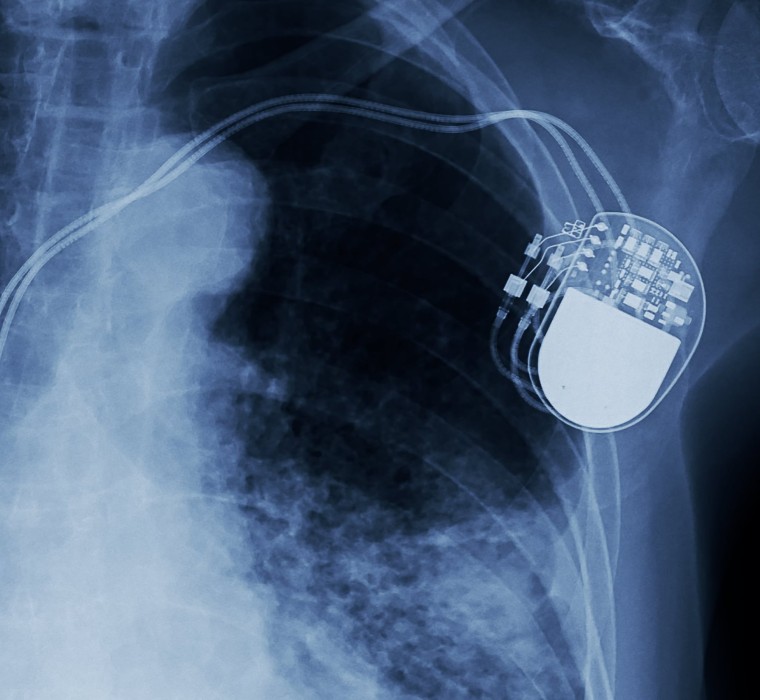
Flex and rigid-flex PCBs from Varioprint offer an innovative solution for modern connection technologies. Thanks to their high versatility and reliability, they have established themselves in sectors such as aerospace, defence, medical technology and industrial electronics. This technology enables assemblies to be designed more reliably, assembly costs to be minimised and space to be used effectively.
Our flex and rigid-flex PCBs are tailored to your requirements, whether for dynamic bending, space constraints, or continuous flexing stress. They are the ideal choice when it comes to connecting moving components or complex geometries. Varioprint stands for the highest quality – from prototypes to series production.
Our experienced engineering team supports you in every phase of your project and helps to realise your requirements efficiently and precisely. Rely on Varioprint for reliable and innovative flex and rigid-flex PCB solutions.
Range of services
Structure and technology
Multilayer circuits with symmetrical and asymmetrical design, semi-flex (static bending cycles for assembly) and full-flex design (for dynamic bending cycles) in a wide range of materials
Blind vias, buried vias, µvias with and without copper filling as well as plugged via with/without overplating
Dimension and formats
Thickness 0.1 mm to 4.8 mm thickness
Panel formats used
305x460 mm and 460x610 mm
Usable area up to 420x69 mm
Coatings and additional prints
Photosensitive solder mask in various colours using spray and screen printing processes
Solder mask registration
Standard: +–50 µm
Special: +–25 µm
Additional coatings such as labelling print, peel-off mask and carbon print
Circuit pattern structuring
Copper claddings from 18 µm to 210 µm
Conductor widths and spacing
Standard: 75 µm/100 µm
Special: 50 µm/50 µm
Mechanical processing
Contour milling
Deep routing
Scoring
Laser processing
Annular rings
Standard: 100 µm
Special: 75 µm
Materials
Tg 135 °C and high Tg 170 °C FR4
Halogen-free materials
PTFE materials
Polyimides (Kapton) and special materials such as LCP (liquid crystal polymers)
End surfaces
Various chemical and galvanic gold surfaces as well as chemical tin and silver surfaces or pure organic protective lacquers
Electroplating and copper plating
Aspect ratio up to 1:12 with 0.15 mm drill diameter
1:15 with 0.3 mm drill diameter
Copper in vias according to IPC 2, IPC 3 or customised