High-frequency PCBs, precision and innovation for the highest demands
We are one of the leading global suppliers in the manufacture of high-frequency PCBs. Our expertise includes the production of multilayer circuits made of Teflon (PTFE), which can be manufactured using fusion bonding, as well as constructions with mixed materials such as FR4 and PTFE. Embedded heatsinks and stably controlled process parameters are standard for us to guarantee consistently high quality – even with high production volumes.
In close cooperation with renowned material suppliers such as Rogers, Taconic and Neltec, we offer a unique range of services for your high-frequency applications. Our specialist engineering team supports you in the selection of suitable materials and in the structure and design of your PCB.
For sophisticated high-frequency solutions between 77–79 GHz, especially for applications such as radar systems in the mobility industry, we offer customised processes that guarantee the highest RF performance and maximum reliability. Rely on our expertise and power of innovation to realise your high-frequency performance requirements at the highest level.
Range of services
Structure and technology
Multilayer and mixed structure circuits, PTFE fusion bonding, heatsink technology and pure PTFE softboards
Blind vias, buried vias, µvias with and without copper filling as well as plugged bore holes with/without overplating
Dimension and formats
Thickness 0.2 mm to 4.8 mm thickness
Format up to 569x490 mm
Used panel formats 460x610 mm and 530x610 mm
Coatings and additional prints
Photosensitive solder mask in various colours using spray and screen printing processes
Solder mask registration
Standard: +–50 µm
Special: +–25 µm
Additional prints such as labelling print, peel-off mask and carbon print
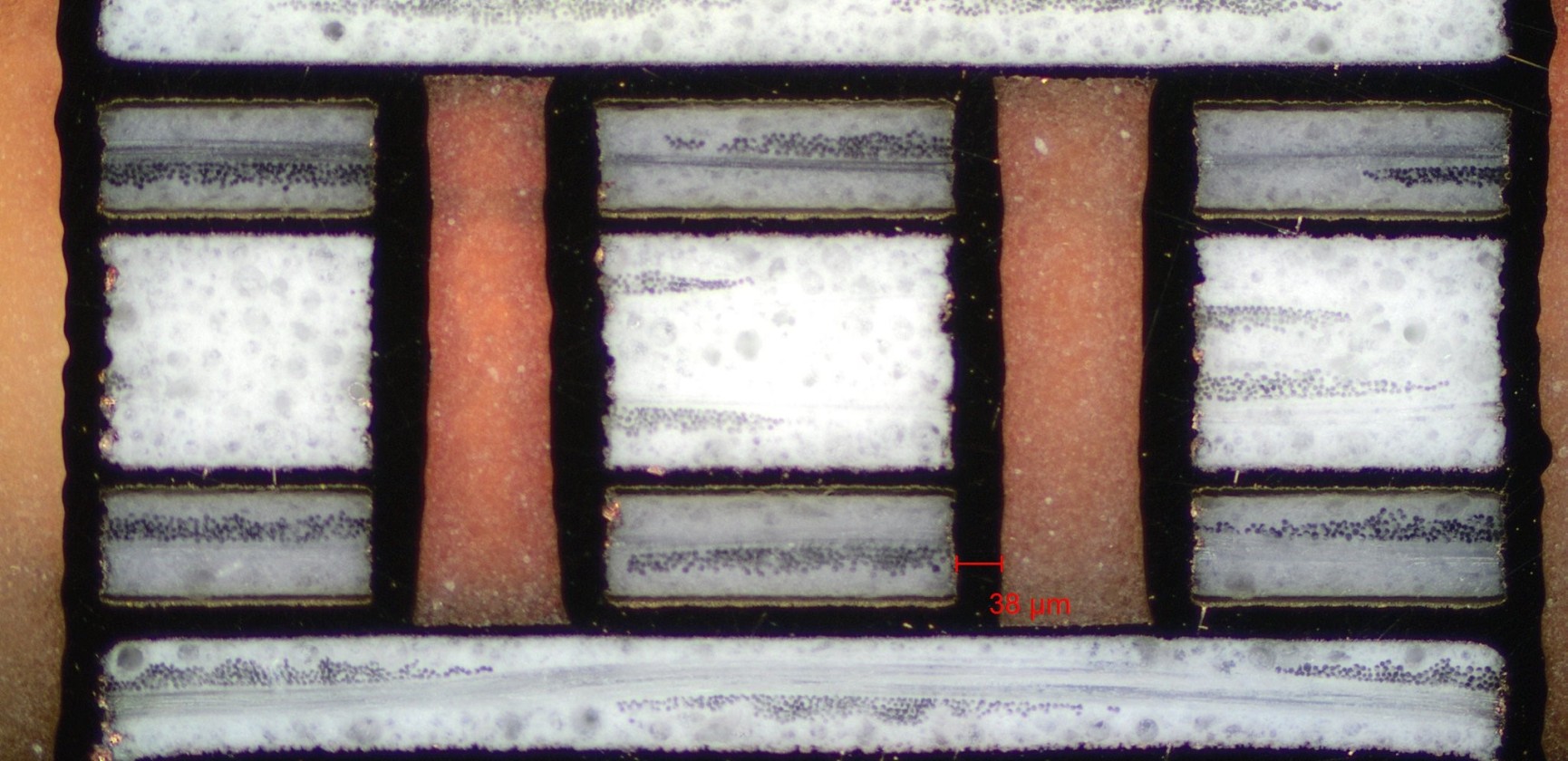
Circuit pattern structuring
Copper claddings from 18 µm to 210 µm
Conductor widths and spacing
Standard: 75 µm/100 µm
Special: 50 µm/50 µm
Etching tolerances
Standard: +–20 µm
Special +–10 µm
Mechanical processing
Contour milling
High-precision deep routing for cavities and waveguide connections
Scoring
Laser processing
Annular rings
Standard: 100 µm
Special: 75 µm
Materials
HF substrates from all common manufacturers such as Rogers, Taconic, Neltec or Isola, e.g. RO3003 or NY-9220 as well as many other materials
In addition to core materials, all common HF bondplies such as RO4450, Gore Speedboard or Taconic Fastrise can also be laminated
End surfaces
Various chemical and galvanic gold surfaces as well as chemical tin and chemical silver surfaces and pure organic protective lacquers
Nickel-free surfaces are also available, which are particularly important for HF technology
Electroplating and copper plating
Aspect ratio up to 1:12 with 0.15 mm drill diameter
1:15 with 0.3 mm drill diameter
Copper in vias according to IPC 2, IPC 3 or customised
Thanks to state-of-the-art electroplating processes, very even copper distribution on the panel and thus a precise etching tolerance is achieved