Single-sided and double-sided PCBs, proven classics with state-of-the-art technology
Single-sided and double-sided PCBs are one of the cornerstones of electronics production and at the same time offer impressive possibilities for precise and innovative applications. Varioprint combines traditional designs with the latest manufacturing technologies to fulfil even the highest demands.
With ultra-fine conductor structures down to 50 µm, controlled depth drilling and precise milling or laser techniques, we create solutions that are perfectly customised to your individual requirements. Our wide range of materials and complex mechanical processing enable a wide variety of applications – from standard applications to highly specialist designs.
Challenges are what drives us. Our experienced team of engineers, polymechanics and galvanic technicians is ready to turn your demanding specifications into high-quality solutions. Varioprint, your partner for single-sided and double-sided PCBs at the highest level.
Range of services
Structure and technology
Single-sided and double-sided PCBs with/without via in a wide range of materials
Dimension and formats
Thickness 0.2 mm to 4.8 mm thickness
Panel usage up to 569x490 mm
Coatings and additional prints
Photosensitive solder mask in various colours using spray and screen printing processes
Additional coatings such as labelling print, peel-off mask and carbon print
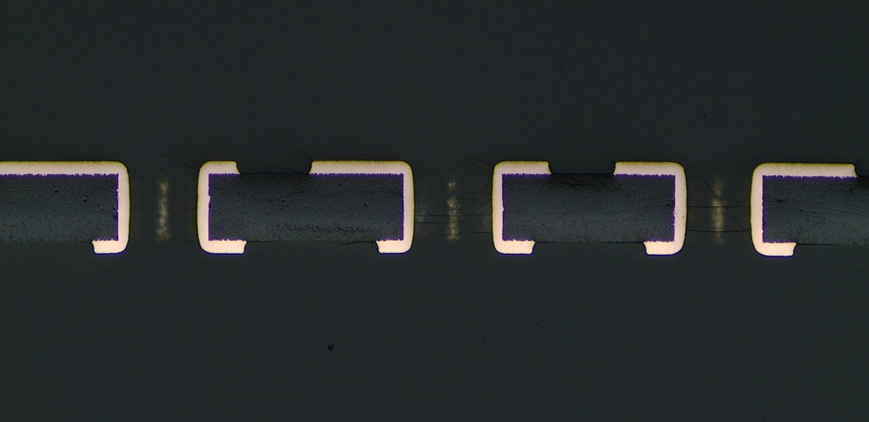
Circuit pattern structuring
Copper claddings from 18 µm to 210 µm
Conductor widths and spacing up to 50 µm/50 µm
Mechanical processing
Contour milling
Deep routing
Scoring
Laser processing
Complex contour machining or demanding deep routing work can be carried out with maximum accuracy and high efficiency
Materials
FR4, Tg 135 °C with filler
FR4 high Tg 170 °C
Halogen-free materials
PTFE materials
Special materials
End surfaces
Various chemical and galvanic gold surfaces as well as chemical tin and silver surfaces and pure organic protective lacquers
Special surface requirements, such as partial hard gold on ENIG, are just one example of the large portfolio
Electroplating and copper plating
Aspect ratio up to 1:12 for 0.15 mm drill diameter and 1:15 for 0.3 mm drill diameter, copper in the bore holes according to IPC 2 (min. 15 µm–20 µm), IPC 3 (min. 25 µm) or customised