Multilayer and HDI PCBs, high-precision solutions for state-of-the-art electronics
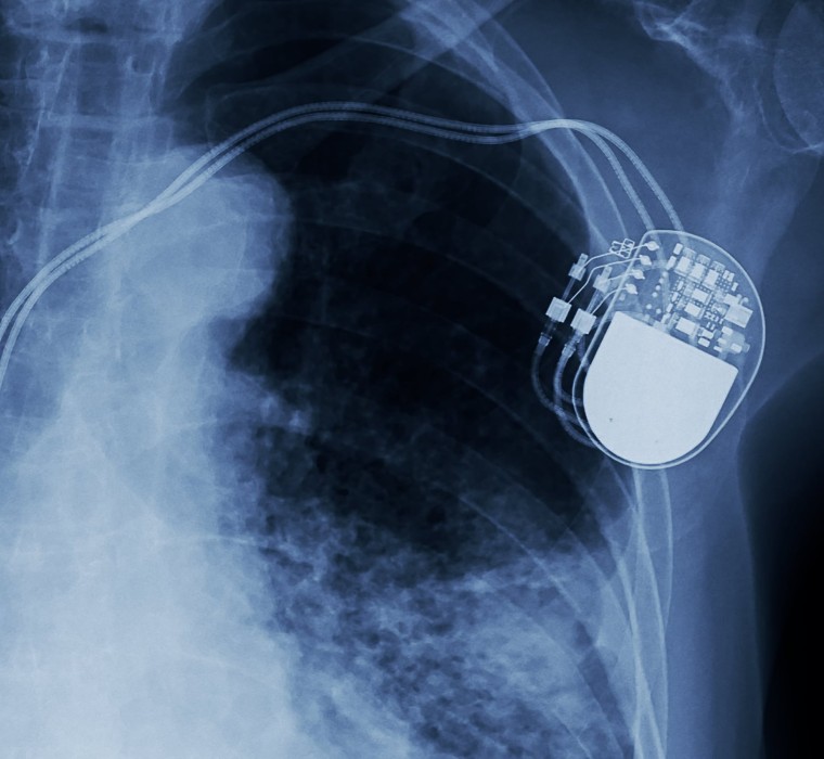
Multilayer and HDI PCBs from Varioprint are the answer to increasing demands for miniaturisation, high packing densities and optimised signal integrity. With over 35 years of expertise in multilayer circuit manufacturing, we offer products that guarantee the highest quality and reliability. Thanks to optimised automated processes, precise registration and state-of-the-art via technologies, our PCBs meet the most demanding technical requirements.
The development of ultra-thin cores with a thickness of just 50 µm, ultra-fine structures and an increasing number of layers make our multilayer and HDI solutions the standard for modern assemblies. Our PCBs efficiently separate analogue and digital areas and enable maximum functionality in the smallest possible space thanks to integrated blind and buried vias as well as copper-filled µvias.
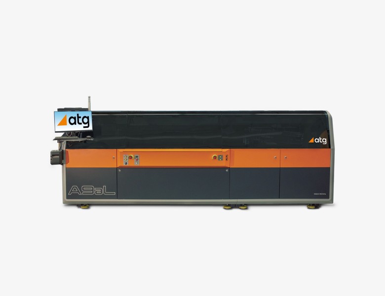
With our high-precision laser drilling systems and our state of the art vertical electroplating equipment, we offer maximum process stability and highest quality standards. Varioprint stands for innovation and expertise in the development of multilayer and HDI PCBs that fulfil tomorrow's requirements today.
Range of services
Structure and technology
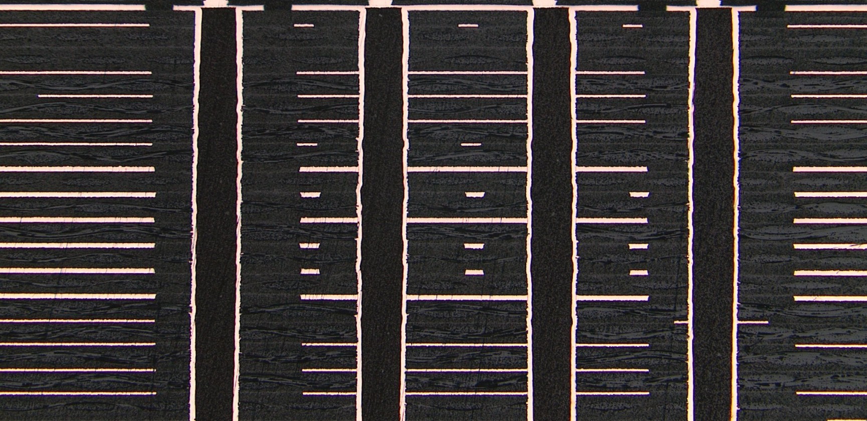
Multilayer and HDI circuits of up to 28 layers with a wide range of materials
Blind vias, buried vias, µvias with and without copper filling as well as plugged bore holes with/without vias
Dimension and formats
Thickness 0.2 mm to 4.8 mm thickness
Panel usage up to 569x490 mm
Used panel formats 460x610 mm and 530x610 mm
Coatings and additional prints
Photosensitive solder mask in various colours using spray and screen printing processes
Solder mask registration Standard: +–50 µm Special: +–25 µm possible
Additional coatings such as labelling print, peel-off mask and carbon print
Circuit pattern structuring
Copper claddings from 18 µm to 210 µm
Conductor widths and spacing
Standard: 75 µm/100 µm
Special: 50 µm/50 µm possible
Mechanical processing
Contour milling
Deep routing
Scoring
Laser processing
Remaining rings
Standard: 100 µm
Special: 75 µm
Materials
FR4, Tg 135 °C fillers
FR4 high Tg 170 °C
Halogen-free materials
PTFE materials
Special materials
Standard glass fabric type 106/1080/2116 and 7628, others available, depending on requirements and structure
End surfaces
Various chemical and galvanic gold surfaces as well as chemical tin and silver surfaces and pure organic protective finishes
Electroplating and copper plating
Aspect ratio up to 1:12 with 0.15 mm drill diameter, 1:15 with 0.3 mm drill diameter
Copper in vias according to IPC 2, IPC 3 or customised