The needs for custom-designed, high-end printed circuit boards for demanding applications are constantly increasing. To meet the growing demands for precision, reliability, and flexibility – and to continue serving our customers as a trusted technology partner in the future – Varioprint has made targeted and comprehensive investments in new machinery and technologies.
These investments are specifically designed to meet the growing demands of our customers in the industrial, aerospace & defense, and medical sectors. The key drivers are trends toward miniaturization, complex structures, and high-frequency applications, combined with increasing customer requirements for high registration accuracy, flexible manufacturing, increased production capacity, and stable process capability across a growing number of lamination cycles.
They cover five key areas of manufacturing – electronic testing, drilling and milling, trimming of laminated multilayers, and solder mask exposure – and enable us to both increase our capacity in mechanical machining and further expand our capabilities in miniaturization, complex structures, and high-frequency applications.
Our customers can benefit from this regardless of batch size: whether it’s a prototype or mass production, a standard design or a wide variety of variants, Varioprint offers the right solution. In this article, we explain what this means in concrete terms and what added value we offer our customers through these capital investments.
Electronic Testing: Greater Coverage, Greater Security
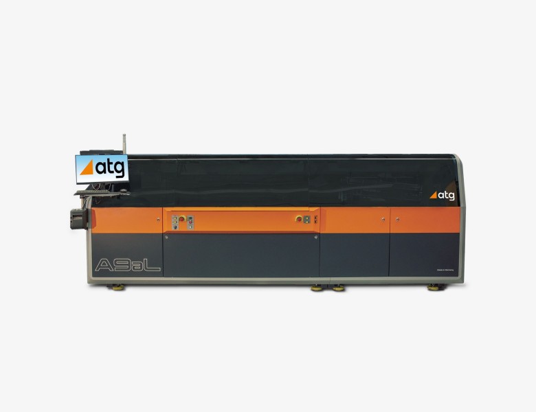
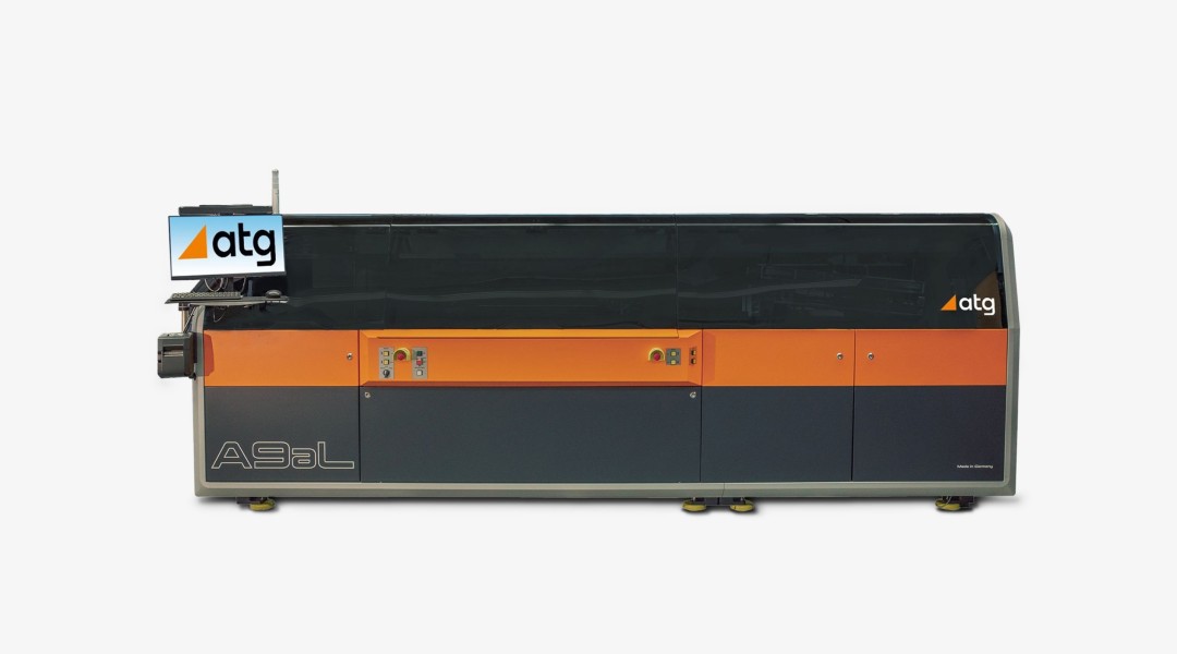
With the new ATG A9aL, we are leveraging state-of-the-art flying-probe technology. This testing method is particularly well-suited for high-mix and low-to-medium-volume production and enables the cost-effective testing of a wide variety of variants without the need for complex adapters.
The A9aL significantly expands our defect detection capabilities, particularly for complex HDI, flex, and rigid-flex printed circuit boards. Key test functions include the detection of open circuits and short circuits, HiPOT high-voltage tests, Kelvin 4-wire measurements for very low resistances, and backdrill tests. In addition, pads as small as approximately 50 µm can be reliably tested.
Thanks to the expanded test coverage, the testability of fine-pitch and HDI designs, and the integrated additional test methods, our first-pass yield increases measurably. New designs can be programmed within a few hours and tested on the same day. For serial production, the system also offers a high degree of automation with automatic loading.
Drill: Maximum precision for complex HDI designs
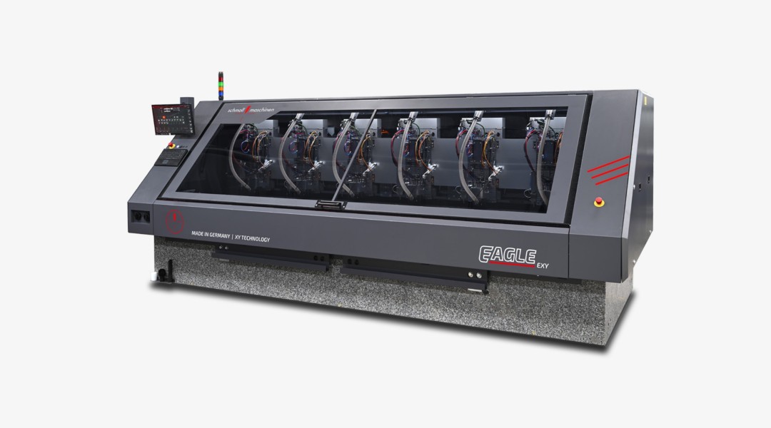
The new Schmoll EXY-5 Eagle series is specifically designed for high-precision HDI and backdrill applications. It offers significant improvements in the machining of thin cores, materials prone to warping, high-speed materials with tight tolerances, and complex HDI structures requiring multiple pressing cycles. Drill diameters ranging from 0.050 mm to 6.25 mm are possible, and aspect ratios from 10:1 to 14:1 can be reliably achieved, depending on the material, drill diameter, copper thickness, and overall structure.
The system operates with individual XY tables, individual CCD camera registration per station, and station-specific shrinkage and expansion values. This enables accuracies in the range of ±20 µm. For HDI designs, this means smaller capture pads, narrower resist ring widths, tighter trace and drill tolerances, and more stable via-in-pad and sequential lamination processes.
Via quality improves noticeably, as the vacuum and spindle speed—ranging from 20,000 to 220,000 RPM—are optimally tuned for small drill diameters. Since the system was specifically developed for high-layer-count boards, back-drill applications, numerous drilling cycles, and multiple registration steps, complex multilayer PCBs in particular benefit from consistent precision over long operating periods and improved repeatability after multiple lamination cycles.
Milling Machine: Greater Flexibility for Complex Designs
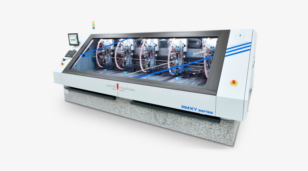
The new Schmoll Raptor RMXY-6 is designed for high-precision contour and depth milling and enhances our capabilities, particularly with regard to complex internal contours, depth milling and cavities, rigid-flexible transitions, HF and backdrill geometries, as well as very tight positional tolerances across multiple machining steps. Thanks to high-precision depth control, depth milling tolerances of up to approximately ±15 µm are possible.
Similar to a drilling machine, the RMXY-6 operates with individual XY tables, CCD camera registration per station, and station-specific compensation, enabling standard accuracies of ±25 µm.
For high-frequency and high-speed printed circuit boards, the machine offers several key advantages: more precisely defined contours and cavities, cleaner milled edges for more stable RF characteristics, and improved backdrill capabilities with reproducible stub lengths and reduced signal reflections. Customers with technologically demanding designs also benefit from expanded capabilities for special geometries, smaller inner radii, and complex rigid-flex contours.
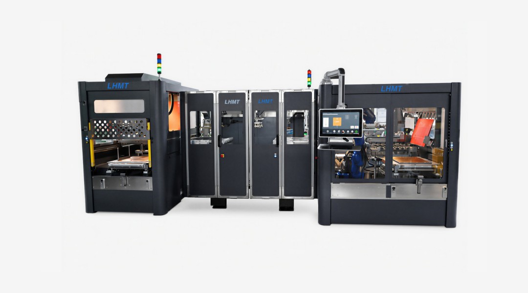
Trimming Machine: Quality Starts at the Edge
The new LHMT MBM 2.0 is designed for high-precision edge processing of printed circuit boards after lamination. Controlled trimming is a key quality factor, particularly for thin or thick materials, rigid-flex products, HDI boards, boards with a high copper content, and metal-core products.
Controlled trimming reduces mechanical stress, localized material strain, microcracking, and potential delamination at the outer edges. This has a direct positive impact on the quality of downstream internal production processes.
The MBM 2.0 also stands out for its high degree of automation, high process stability, fully automated process control of thickness and copper cladding, as well as short programming, setup, and changeover times. The result is efficient production and consistently high quality, even for large production runs and complex panels.
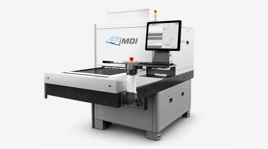
Exposure Unit and UV Curing Oven: Ultra-fine Structures for State-of-the-Art Components
The new Schmoll MDI Beam ST with 30-µm exposure heads sets new standards in direct-imaging exposure of solder resist masks. The newly developed Beam technology enables extremely short exposure times with uniform polymerization.
This system allows for the reliable production of solder resist lines ranging from approximately 40 to 50 µm. In addition, it enables small mask apertures, precise pad exposure for fine-pitch components, and defined pad separations in the HDI sector. The camera-based fiducial recognition with individual panel compensation and automatic scaling achieves a registration accuracy of ±15 to 25 µm.
For high-density designs, such as those with BGAs or µBGAs, this means finer solder resist bridges, improved pad clearance, and thus significantly greater design freedom. The more precise and uniform exposure provided by the latest beam technology also improves the adhesion, insulation, and long-term stability of the solder resist mask, even with challenging material formulations.
With these investments, Varioprint highlights its commitment to supporting customers from the initial idea through to a successful market launch.
Whether it’s high-end HDI, high-frequency, rigid-flex, or thick copper: Using state-of-the-art manufacturing technologies and in-depth process expertise, we deliver tailored and reliable solutions for a wide range of requirements.